
Linked Publication
Every photonic chip starts as an idea about light: split it evenly, route it by wavelength, twist it from one mode into another. Turning that idea into a real, etchable pattern of silicon and glass is where things get hard — not because we can’t imagine a shape that does the job optically, but because most of the shapes an algorithm imagines cannot actually be fabricated.
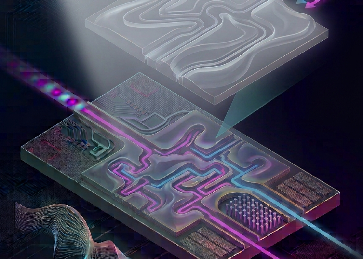
Our new paper, “Intrinsically Design-Rule-Compliant Nanophotonic Inverse Design via Learned Generative Manifolds,” published in Laser & Photonics Reviews, tackles this mismatch head-on. Rather than teaching an optimizer to avoid fabrication violations, we taught it to never be able to draw one in the first place.
The Promise — and the Catch — of Inverse Design#
Inverse design has become one of the most powerful tools in integrated photonics. Instead of hand-sketching a waveguide bend or a splitter, you specify what you want the device to do — split power 50/50, route 1500 nm one way and 1600 nm another — and an optimization algorithm iteratively reshapes a grid of pixels until the simulated response matches that target.
The strange and useful thing about this process is that it is ill-posed: for almost any target response, there isn’t one correct geometry, but an enormous family of them. That sounds like a problem, but it’s actually an opportunity — somewhere inside that huge space of optically-equivalent geometries, there must also exist ones that happen to satisfy a foundry’s fabrication rules: minimum linewidth, minimum spacing, smooth curvature, no impossibly small islands or gaps.
The catch is that conventional optimization has no built-in sense of where those compliant designs live. It searches blindly across the full space of pixel patterns and has to be steered toward fabrication compliance from the outside.
Patching the Rules on From the Outside#
The standard fix is to bolt a regularization term onto the optimization objective — a penalty that nudges pixel values toward fully solid or fully empty, smooths boundaries, and discourages tiny disconnected features. In practice, this is implemented through scheduled projection filters: a parameter (often called β) is slowly cranked up over hundreds of iterations, progressively forcing a blurry, grayscale pattern into a crisp black-and-white layout.
It works — but not gracefully. Every time β is stepped up, the optimization landscape effectively changes, and the loss function jumps before it can settle again. On a benchmark 50/50 power splitter, for instance, this conventional approach only reaches a fully discrete, well-defined layout at the very last of 800 iterations, with visible spikes in the loss curve each time the discretization strength is ratcheted up.
Beyond the instability, this approach demands careful hyperparameter tuning — how fast to schedule β, when to start, how strong the boundary penalty should be — and that tuning is often specific to a single foundry’s design rules. Change the fabrication platform, and the schedule may need to be rediscovered.
A Different Idea: Redesign the Search Space Itself#
Our starting question was simple: what if fabrication compliance wasn’t something we enforced during the search, but something built into the space being searched?
Formally, conventional inverse design explores an ambient design space of all possible pixel patterns, and only a small subset of that space is actually fabrication-compatible. Regularization tries to steer the optimizer toward that subset from outside. We instead constructed a generative manifold — a low-dimensional latent space, mapped through a trained neural network generator, whose every single output is guaranteed to sit inside the fabrication-compatible subset.
Once compliance is guaranteed by construction, the optimization problem collapses to something much simpler: adjust the latent input until the generated device’s simulated response matches the target. No penalty term. No schedule. No hyperparameter babysitting.
Building a Network That Can Only Draw Compliant Chips#
Making that guarantee real required designing a generator that is architecturally incapable of producing a design-rule violation. Our network takes a small, low-dimensional array as input and passes it through cascaded upsampling stages, a handful of upsampling-convolution layers with softmax nonlinearities, a scheduled thresholding step, and a final morphological closing operation that removes any stray gaps or islands below the minimum feature size. Because the final thresholding step isn’t naturally differentiable, we use a straight-through estimator to keep gradients flowing during training.
We trained this generator on a custom dataset of smoothly-varying Perlin-noise inputs — chosen because they produce a rich mix of large and small geometric features — using a topological loss function that directly penalizes minimum-width and minimum-spacing violations. Over the course of training, this design-rule-check loss falls by more than four orders of magnitude, and the length-scale violations visible early in training disappear one by one as the network converges. Small islands and holes are cleaned up automatically by the morphological closing step, and boundary regions and waveguide junctions are explicitly exposed to this loss during training so that compliance holds all the way to the edges of the device, not just in its interior.
Because the whole generator is fully convolutional, it is size-agnostic: a single trained model can generate devices of essentially any footprint just by changing the size of its latent input, with no retraining required.
One Generator, Two Rulebooks#
Different fabrication processes come with different minimum feature sizes — electron-beam lithography (EBL) can resolve features down to about 60 nm, while photolithography (PL), though cheaper and more scalable, is typically limited to around 150 nm. Rather than building a new regularization scheme for each, we simply trained two versions of the generator with different upsampling ratios and convolution kernel sizes: a finer-grained EBL model with more, smaller upsampling-convolution stages, and a coarser PL model with fewer, larger-kernel stages that naturally produce chunkier, more conservative geometries. Both networks are trained once and then reused across arbitrary device footprints.
Putting the Manifold to Work#
We tested the framework on a broad set of representative silicon photonic devices spanning the 1500–1600 nm band on a 220-nm single-etch SOI platform.
Broadband power splitters. For a benchmark 50/50 splitter, the generator-based approach converged in 149 iterations, versus 800 iterations for the conventional pixel-based method — over five times faster — while remaining fully discrete throughout, rather than gradually solidifying. We then pushed the same generator to design splitters with arbitrary ratios: a 30/70 splitter (0.11 dB simulated insertion loss) and a 10/90 splitter (0.09 dB), both converging in 150 iterations and holding their target splitting ratios steadily across the full 1500–1600 nm band. A symmetry-constrained variant of the 50/50 splitter converged in just 110 iterations with an insertion loss of 0.067 dB.
Wavelength duplexer. For a device that must route short wavelengths to one port and long wavelengths to another, the generator-based design reached 94% peak transmission (0.25 dB insertion loss) after 160 iterations, cleanly separating the 1500–1550 nm and 1550–1600 nm bands into its two output ports.
Mode converter. Converting the fundamental TE₀ mode into the first-order TE₁ mode — a much smaller, simpler design task — converged in 130 iterations to a simulated insertion loss of just 0.03 dB, in a footprint of only 2.1 × 2.1 μm², maintaining 98–100% conversion efficiency across the full simulated bandwidth.
Across all of these devices, we also stress-tested robustness by simulating ±15 nm over- and under-etching, and transmission stayed within acceptable bounds of the as-designed performance in every case.
How It Stacks Up#
| Conventional pixel-based optimization | Our generative manifold | |
|---|---|---|
| Where fabrication rules live | Bolted on as an external penalty term | Built into the geometry the generator can produce |
| How discreteness is reached | Gradually, via scheduled projection-strength (β) increases | Immediately — every output is already discrete |
| Hyperparameter tuning | Required per device, per fabrication platform | None beyond training the generator once |
| Iterations to converge (50/50 splitter) | 800 | 149 (5.3× fewer) |
| Portability across platforms | Regularization often re-derived per foundry rule set | Swap generator (EBL ↔ PL) by adjusting resolution/kernel size |
We also benchmarked our simulated results directly against previously reported inverse-designed devices satisfying comparable design rules:
| Device | Best previously reported IL (dB) | Our EBL result (dB) | Our PL result (dB) |
|---|---|---|---|
| Power splitter | 0.24 – 0.46 | 0.06 | 0.22 |
| Wavelength duplexer | 0.62 – 1.17 | 0.25 | 1.19 |
| Mode converter | 0.24 – 0.64 | 0.03 | 0.10 |
(IL: simulated insertion loss. Minimum feature sizes among compared works range from roughly 70 nm to commercial foundry specifications; ours are 60 nm for EBL and 150 nm for PL.)
This comparison also came with an honest caveat. In a separate head-to-head test on a 150-nm photolithography-compatible duplexer, our generator-based method converged 4.5 times faster than the pixel-based baseline (250 vs. 1,116 iterations) — but the pixel-based method ultimately reached a marginally lower loss and a somewhat better spectral extinction ratio (14–21 dB vs. 10–14 dB). Confining the search to a learned, compliant manifold trades a small amount of final-performance ceiling for a large gain in convergence speed and robustness — a trade-off that held consistently across the device types we tested comparatively.
Where the Rules Still Need Work#
Our current topological loss enforces a single, spatially uniform minimum feature size across the whole device — appropriate for standard single-etch waveguide platforms governed by one foundry rule set, but not yet suited to structures that mix length scales within a single device, such as nanocavities with sub-10-nm confining features embedded in an otherwise conventionally-sized surrounding structure. Extending the framework to such cases would mean replacing the global thresholds with spatially-varying ones and giving the generator a multi-branch architecture that can handle fine and coarse features separately — a natural next step.
It’s also worth being clear about what this paper does and does not show: every performance number reported here comes from electromagnetic simulation (FDFD), not from a fabricated and measured device. Experimental validation is the vital next step to confirm these simulated metrics translate to real chips.
What This Opens Up#
Because the electromagnetic solver and the generator are fully decoupled — connected only through gradient flow, with no shared assumptions about resolution or discretization — the simulation engine underneath this framework can be swapped for any differentiable solver suited to a given device or platform, from 2D-FDFD to 3D-FDTD or EME. And because compliance is a property of the generator rather than the optimization loop, adapting to a new fabrication process is a matter of retraining one lightweight network rather than re-deriving a regularization schedule.
Taken together, this points toward a genuinely platform-agnostic inverse design pipeline: specify a target response, pick the fabrication process, and let the optimization run in a space where every candidate design is already buildable. The trained model weights and code for both the EBL and PL generators are openly available, and we hope they serve as a practical starting point for groups looking to bring similar guarantees to their own design workflows.
In short: by moving fabrication constraints from an external penalty into the structure of the search space itself, this work removes the need for scheduled regularization in nanophotonic inverse design — converging up to 5× faster while matching or exceeding the best previously reported simulated performance across power splitters, wavelength duplexers, and mode converters.
Code & Data#
The trained EBL and PL generator models are publicly available at github.com/Photonic-Architecture-Laboratories/drcgenerator.
This work was supported by the Scientific and Technological Research Council of Turkey (TÜBİTAK), grant number 122E214.
Citation#
@article{danis2026lpor,
  author  = {Danis, Bahrem Serhat and Desdemir, Demet Baldan and Akcakoca, Enes and
             Yanmaz, Zeynep Ipek and Polat, Gulzade and Dasdemir, Ahmet Onur and
             Aydogan, Aytug and Magden, Abdullah and Magden, Emir Salih},
  title   = {Intrinsically Design-Rule-Compliant Nanophotonic Inverse Design via
             Learned Generative Manifolds},
  journal = {Laser \& Photonics Reviews},
  year    = {2026},
  pages   = {e71486},
  doi     = {10.1002/lpor.71486},
  url     = {https://onlinelibrary.wiley.com/doi/abs/10.1002/lpor.71486}
}
#NanophotonicsInverseDesign #SiliconPhotonics #GenerativeModels #IntegratedOptics #FabricationAwareDesign #PhotonicArchitectureLaboratories