Linked Publication
As our digital world demands more speed and smarter sensors, the hardware under the hood—Photonic Integrated Circuits (PICs)—must become increasingly complex. But there’s a catch: designing these tiny chips to handle light in specific, ultra-fast ways is notoriously difficult and computationally expensive.
Traditionally, engineers relied on physical intuition or slow, iterative simulations that could take hours or even days to design a single component. In a new study published in Nature Communications, PAL researchers have unveiled a workaround: a Highly-Scalable Deep Photonic Network platform that can design state-of-the-art optical components in under two minutes.
The Challenge: Beyond Human Intuition#
Think of light as a messenger that needs to be split, merged, or filtered with perfect precision. While we’ve mastered simple “light-splitters” for years, modern applications like quantum computing and medical sensing require “arbitrary” functionality—meaning the chip needs to do exactly what a specific application requires, over a wide range of wavelengths.
Designing these “perfect” chips usually requires massive supercomputing power. The larger the design, the more “degrees of freedom” there are, and the simulation math becomes a bottleneck.
The Solution: A Mesh of Light#
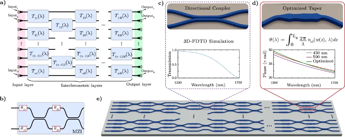
The PAL team’s breakthrough involves a mesh-like architecture of Mach-Zehnder interferometers (MZIs). By treating this physical mesh like a Deep Learning Network, the researchers created a “design platform” where the physics are built right into the model.
Instead of guessing and checking, the platform uses physics-informed machine learning to optimize the waveguide geometry. This allowed the team to design:
- Ultra-broadband 50/50 and 75/25 power splitters (essential for routing data).
- Spectral duplexers (for separating different signals).
The result? All three devices were designed in less than two minutes and matched or exceeded state-of-the-art experimental performance when fabricated on standard silicon-on-insulator chips.
Why It Matters#
This isn’t just about speed; it’s about scalability. By making complex photonic design “tractable” (meaning we can actually do the math in a reasonable amount of time), this platform opens the door to:
- High-throughput communications (faster data transfer).
- Quantum information processing (the next frontier of computing).
- Medical and biological sensing (more accurate diagnostics).
“This framework provides a path towards the systematic design of large-scale photonic systems,” says the team. By merging the principles of deep learning with the physics of light, we are moving closer to a future where high-performance optical chips are limited only by our imagination, not our computing power.