Linked Publication
We’re thrilled to share that our latest work, “Experimental Demonstration of Ultra-Wideband Tapers, Splitters and Crossings with sub-0.1dB Loss Through Computationally Efficient and Data-Driven Eigenmode Expansion” has been accepted for presentation at CLEO Europe 2025!
Rethinking Simulation Speed#
Photonic devices like tapers, splitters, and crossings are foundational to modern optical systems—but traditionally, designing them with high accuracy and low loss comes at a heavy computational cost.
This work presents an alternative: a data-driven eigenmode expansion (EME) framework that reduces simulation times from hours to milliseconds—without sacrificing physical accuracy. By leveraging precomputed eigenmode scattering matrices and parallel GPU processing, we model broadband light propagation in arbitrary geometries with remarkable speed.
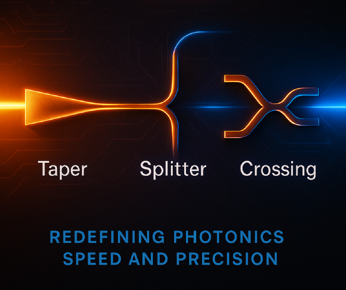
The Devices#
We designed and fabricated three fundamental photonic components on a silicon platform:
- Taper (30 µm): < 0.050 dB insertion loss
- 1×2 Splitter (2 µm): < 0.083 dB insertion loss
- Crossing (12×12 µm²): < 0.051 dB insertion loss
All devices operate with sub-0.1 dB losses across 1500–1580 nm, offering over 250 nm of 1 dB-bandwidth. These performances were verified through 3D-FDTD simulations and cutback measurements on cascaded devices.
Why It Matters#
- Speed: The design times were just 18s for the taper, 14s for the splitter, and 5s for the crossing—that’s over 100,000× faster than conventional EME.
- Accuracy: Comparable to full 3D-FDTD methods.
- Flexibility: Waveguide widths and device lengths can be customized as design hyperparameters.
This framework opens new doors for rapid, application-driven photonic design—from optical interconnects to on-chip sensing and computing.
What’s Next?#
We aim to expand this approach to:
- Fabrication-tolerant and lithography-aware design
- Multi-layer and non-planar geometries
- AI-accelerated hybrid models for even faster design exploration
See you at CLEO Europe 2025 in Munich!
#SiliconPhotonics #CLEOEurope #IntegratedOptics #OpticalDesign #EME #SimulationSpeed