PAL members are heading to San Francisco for SPIE Photonics West 2026!
We are excited to share our latest breakthroughs in integrated photonics and optical computing. This year, we have three oral presentations and two posters covering
Design Rule-Compliant Inverse Design: Using deep generative networks for fabrication-compatible devices AI-Driven Optimization: Transformer-based surrogate simulator models complex photonic architectures Thermally Reconfigurable Devices: Novel reconfigurable splitters and adaptive photonic circuits Random Deep Photonic Processors: High-throughput optical inference with cascaded MZI arrays Photonic Imitation Learning: Deep photonic agentic networks for control tasks Our work at this conference focuses on enabling arbitrary optical capabilities through deep photonic network architectures and AI-enabled devices.
We look forward to seeing you there!
Integrated photonics has always had a complicated relationship with polarization. The conventional solution has been polarization-diversity schemes: separate the two polarizations and route them through duplicate circuits—doubling both footprint and complexity.
We decided to flip the script. Instead of duplicating circuits, we treat polarization as just another parameter to program directly into the geometry of our devices, just like we do for wavelength.
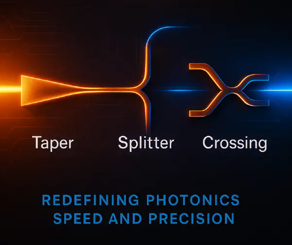
We’re thrilled to share that our latest work, “Experimental Demonstration of Ultra-Wideband Tapers, Splitters and Crossings with sub-0.1dB Loss Through Computationally Efficient and Data-Driven Eigenmode Expansion” has been accepted for presentation at CLEO Europe 2025!
Rethinking Simulation Speed # Photonic devices like tapers, splitters, and crossings are foundational to modern optical systems—but traditionally, designing them with high accuracy and low loss comes at a heavy computational cost.
This work presents an alternative: a data-driven eigenmode expansion (EME) framework that reduces simulation times from hours to milliseconds—without sacrificing physical accuracy. By leveraging precomputed eigenmode scattering matrices and parallel GPU processing, we model broadband light propagation in arbitrary geometries with remarkable speed.
What if you could simulate a photonic device in milliseconds instead of minutes or hours?
This is no longer just an idea. With our recently published design framework ROMEO (Rapid Optical Eigenmode Optimizer), we’re beginning to see what’s possible when simulation times are drastically reduced.
As photonics continues to expand into new applications, there’s growing demand for ultra-efficient, compact, and broadband photonic devices. Algorithmically optimized (or inverse-designed) structures offer a promising approach, but the physical simulations required often dominate the computational cost. To make meaningful progress, we need much faster (and still accurate) simulation techniques. That’s where ROMEO comes in.
We are proud to announce that Prof. Magden has been selected for the highly competitive 2247-D National Early-Stage Researchers Program Award, to support his research on integrated photonic machine learning systems.
This program supports high-impact research projects that aim to fill critical gaps in their fields, offer fresh perspectives to the research community, and hold strong potential for major discoveries and technological breakthroughs. Prof. Magden’s project stands out for its innovative approach to developing photonic hardware that dramatically improves energy efficiency, scalability, and noise tolerance in machine learning systems.
We are pleased to announce that Bahrem Serhat Danis and Ujal Rzayev have joined the Photonic Architecture Lab. Their addition brings new energy and perspectives to our ongoing research in integrated photonics and computational photonic systems. We are excited to have them on board and look forward to the advancements their work will bring.
Bahrem Serhat Danis will focus on research at the intersection of photonic networks and neuromorphic computing. His work aims to explore emerging architectures that leverage the unique capabilities of photonic systems for information processing. He will also contribute to the development of more effective strategies for inverse design.
As our digital world demands more speed and smarter sensors, the hardware under the hood—Photonic Integrated Circuits (PICs)—must become increasingly complex. But there’s a catch: designing these tiny chips to handle light in specific, ultra-fast ways is notoriously difficult and computationally expensive.
Traditionally, engineers relied on physical intuition or slow, iterative simulations that could take hours or even days to design a single component. In a new study published in Nature Communications, PAL researchers have unveiled a workaround: a Highly-Scalable Deep Photonic Network platform that can design state-of-the-art optical components in under two minutes.
PAL members will have a number of presentations at Photonics West this week! We have four oral presentations throughout the week, and also several posters on Wednesday by current and former team members. We look forward to seeing you there.
Most of our work at this conference focuses on demonstrations of photonic design regimes for arbitrary optical capabilities using deep photonic network architectures and AI-enabled devices.
What if the bottleneck in inverse photonic design—solving Maxwell’s equations—could be scaled away?
Our latest work, published in Applied Physics Letters, introduces a multi-faceted factorization caching strategy that drastically reduces simulation runtimes in photonic inverse design. This approach enables up to 9.2× speedups in device optimization, paving the way for efficient design of large-scale, multi-wavelength, and multi-mode nanophotonic devices.
The Challenge in Inverse Design # Adjoint-based optimization has revolutionized the design of nanophotonic devices, enabling automated generation of compact, broadband components with remarkable performance. However, a critical limitation remains: the majority of computation time is spent on solving large sparse linear systems during forward and adjoint simulations.
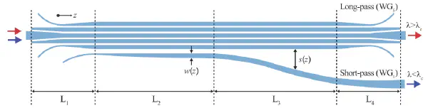
Integrated optical filters are crucial, but achieving truly broadband performance (think >100 nm) with low loss, sharp edges, and design flexibility has been a major hurdle. Rings, MZIs, and AWGs often hit bandwidth ceilings or FSR limitations, while other approaches can be lossy or complex.
What if you could bypass these limits?
In our latest work published in Journal of Lightwave Technology (JLT), we introduce a new way to design and build ultra-broadband silicon photonic filters using adiabatic optimization of coupled waveguides.